


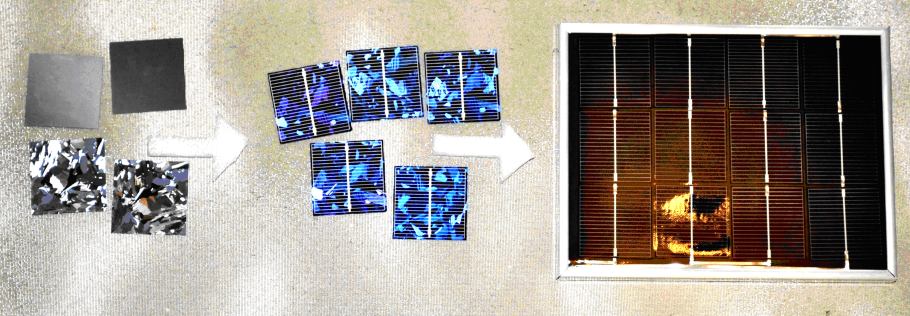
Multicrystalline silicon solar cells
Solar cells - power from the Sun - future for the peopleSolar cell is an electronic device which converts photon energy directly into electrical energy through the photovoltaic (PV) effect without any noise or pollution. This terms refers to a number of types of devices which are generally classified in three generations. The first one are based crystalline silicon with single p-n junction. Three main types of crystalline cells can be distinguished: monocrystalline (Cz-Si), polycrystalline (m-Si) and ribbon sheets. As a push for cheaper PV devices recourse is being made to second generation devices, which benefit from thin-film technology [1]. Since these materials have good light absorption and up to a factor 100 less material is required. Four types of thin-films photovoltaic devices, depending on the active material used are commercially available at the moment: amorphous silicon (a-Si), cadmium telluride, copper indium (gallium diselenide) disulphide and multi junction cells a-Si/Cz-Si knows as HIT structure [2]. These devices, except HIT, are also characterized by a poorer material quality which results in losses of light generated electrons and degradation of efficiency. Third generation solar cells aimed at improving the efficiency of existing devices or introducing different materials and structures. This include multiple junction devices, which combine materials of different spectral responce to cover better the range emitted from the source, mirror or lens based concentrators to increase the level of light exposure, organic polymer and dye-sensitized devices. Some solar cells are designed to operate with concentrated sunlight. The main idea is to use very little of the expensive semiconductor PV material (InGaAs) while collecting as much sunlight as possible with an efficiencies of 40 % under concentrated 200 suns. As the proposed structure, the mechanically stacked triple-junction InGaP-GaAs-Ge with energy band gap of 1.8 eV, 1.4 eV and 0,66 eV respectively, is actively pushing by IMEC [3]. There are several other types of photovoltaic technologies developed today starting to be commercialised or still at the research level, the main ones are: flexible and dye-sensitised solar cells [4]. Based on a similar production process to thin films cells, when the active material is deposited in a thin plastic, the cell can be flexible. This opens the range of applications especially for building integration and end-consumer applications.
The about 90 % of solar cells are produced from crystalline silicon wafers because their technological and ecological clarity and what is more important, the duration stability of output parameters. Moreover, there is considerable momentum behind wafer-silicon PV because it has the largest installed base and largest annual manufacturing capacity. The 100 cm2 solar cells manufactured on the basis of this Si wafer from most producers have over 15 % conversion efficiency - the percentage of power converted from sunlight to electrical energy, measured under standard test condition i.e. light spectrum AM1.5G, normalized to 1000 W/m2 and 25oC cell temperature. This means, that cell has power 1.5 Watt peak what sets its market price. The average sales prices for crystalline Si solar cells are on the level 2.5 Euro/Wp, for modules 3.5 Euro/Wp and the cost for large-scale ground-based or roof-top turnkey systems with crystalline silicon modules is about 5000 Euro/kWp [5]. To satisfy the market demand the main three trends exist nowadays in crystalline Si PV field: a) higher manufacturing throughput with higher conversion efficiencies going from about 15 % to 20 % for industrial cells, b) use of thinner substrates, today 250-300 ľm thin gradually shifting to a thickness of 100 - 130 ľm what determines the specific silicon consumption (SSC) per Wp of solar electricity, c) grows of silicon supply. In mass scale the PV Si solar cells are manufactured into partial or fully automated production lines of between 60 - 100 MWp per year what means about 2000 cells per hour.
Conventionally, photovoltaic materials use inorganic semiconductor allows the formation of charge carrier separating junction. The junction can be either a homojunction, like in Si, or heterojunction with other materials. Ideally, the absorber material of an efficient solar cell should be a semiconductor with bandgap of 1 - 1.5 eV with high optical absorption on the level 104 - 105 cm-1 in the wavelength region of 350 - 1100 nm, a high quantum yield above 90 % for the exited carriers and long diffusion length. When the light falls on a typical semiconductor p-n structure, the light photons of certain wavelengths are absorbed and electrical charge carriers, electron and holes, are generated. These carriers diffuse to the p-n junction where a strong electric field exists, separates the carriers and produces an electric current in the external circuit. This photo-current depends on the incident photon intensity and the nature of semiconductors e.g. band gap energy. For the front side of silicon solar cell, an antireflective coating (ARC) is usually applied before the silver pattern and the silver conductor must penetrate the ARC in order to provide ohmic contact to the doped n-type layer. In order to achieve back contact and back-surface field effect, thick film aluminium are widely used. A single Si crystalline cell produces a current over 30 mA/cm2 and a voltage of about 0.5 volts regardless of its size. If the cells are connected in series the voltage from the cells are added at constant current but if they are connected in parallel, the currents get added at constant voltage level.
The cells which go into the module are interconnected in series and in parallel to get the required power from the module at the specified operating voltage. If more power than can be provided by a single photovoltaic module is required for any application, than a photovoltaic system is designed by linking more modules which number are decided by the power requirement. The daily energy output from PV array will vary depending on its size, orientation and location, season of the year and the daily weather conditions. Energy storage is necessary because the power may be required when sun is not shinning and for this reason specially designed deep-cycle batteries, lead-acid type are employed. The charge controller is placed between the PV array and the storage battery to prevent the battery from being damaged due to overcharging or discharging and to enhance its life. Solar PV systems are broadly classified into three types: stand-alone, hybrid with another form of energy source and grid-connected. Electricity generated from photovoltaic systems produces zero emissions, is modular, and can produce energy anywhere the sun shines. Small stand-along PV systems have proven practical in many areas of country where connection with the local distribution of electricity was too costly or impractical. Such systems, when coupled with storage battery, can serve loads such as homes, radio station, control systems, telephone repeaters and lighting systems.
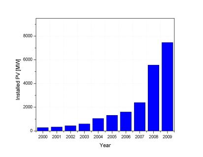
The photovoltaics is a strongly growing industrial and R&D sectors with a annual growth of 40 % over the last decade what can be seen in Fig.1 [6]. The experts believe that it will remain as a result of the efforts made worldwide to reduce dependence on fossil fuel and CO2 emissions related to electricity generation and by a favorable policy through a feed-in tariff. This feed-in tariff is the price for electricity generated from renewable sources, such as solar PV, which national electricity utilities are obliged to buy the electricity. As a result of this sustained growth, the PV sector which measured in 2008 about 20 billion $ in financial terms, will become a plus 100 billion $ sector in 2020. Europe has been leading the global market for PV application. Exemplary in this respect is the decision of the European Commission to go for a share of 20 % renewable energy sources in 2020 in the European energy mix with a share as high as 30 % for electricity generation. This trend, together with the rising importance of the Spanish and Italian markets, have allowed the deployment of more than 1500 MW of photovoltaic installation in Europe, in the year 2007. By far the majority of all the installations are grid-connected. The European market is characterized by a dominant German market while other countries are only recently increasing their importance. In 2007, the German PV industry had a turnover of about 5.7 billion Euro and employed 42600 people. The employment figure for the whole Europe is about 70000 [7]. In Eastern Europe renewable energy still plays a marginal role while the level of solar radiation is no less favourable than in the north of the Germany [8]. In Poland no more than 700 kW of PV systems are today installed mainly as stand-alone systems [9] and in PV sector no more than one hundred people is involved. That situation opens new possibilities for good job and market increase. The PV society meets each year at European and World conferences, exhibitions, fares and events. A lot of books, papers and electronic sites present the latest developments is science, technology and applications of the PV sector.
The PV technology has some unique advantage which allow for many applications for satellites, remote areas, telecommunications, cathodic protection, water pumping, electric fencing, lighting systems, rural electrification, solar home systems, grid-connected systems and miscellaneous applications [10].
Tab.1. Regional distribution of Global and European annual PV market in 2008 [8].
| Global PV market | European PV market |
| Europe 81 % | Spain 56 % |
| Japan 4 % | Germany 33 % |
| USA 6 % | Italy 6 % |
| South Korea 5 % | France 1 % |
| Rest of world 4 % | Rest of Europe 4 % |
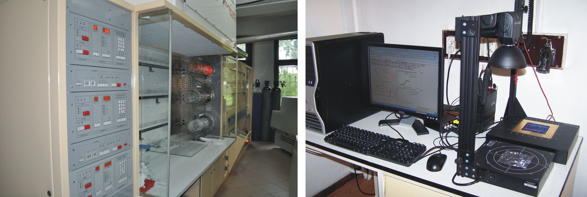
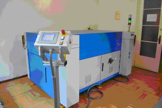
Increasing the cell efficiency is part of our continuous improvement program in the Institute of Metallurgy and Materials Science (IMMS) and we routinely fabricate 12.0 % and 15.0 % efficient cells in our Photovoltaic Laboratory on multi- and monocrystalline Si, respectively. The elaborated technology is simple, inexpensive, verified and has a direct potential for mass scale application [11]. We optimize existing and develop new processing steps for today's and tomorrow's industrial solar cells from raw Si wafers to encapsulated PV modules. The laboratory employs currently 6 people. It bases its work on an technology park including diffusion quartz tube and conveyor belt IR furnaces, screen-printers, evaporator and antireflection deposition system. The staff of PV laboratory has a steady access to transmission and scanning microscopy and X-ray diffractometry, as well as to all research equipment of IMMS. The vacuum laminator in PV laboratory offers closed cycle from silicon wafer to commercial module for R&D, teaching and testing processes.
Extensive measurement systems allow for the characterization of semiconductor and optoelectronic layers, as well as for performance testing of solar cells. The most important are: four point resistivity probe, monochromator, spectrophotometer, sun simulator and life-time photoconductance tester.
The current activities of PV laboratory cover a broad spectrum, ranging from fundamental research to industrial technology transfer like wet chemical processing, diffusion engineering, passivation and metallization processing. The focus of the research projects is not only on standard industrial solar cell but covers the novel materials and effects like thin antireflective layers, quantum structures and laser processing. The laboratory has close links with -several Polish and European research institutes, like for example a well know in PV society the Institut d'Electronique du Solide et des Systemes - CNRS - Universite Louis Pasteur in Strasbourg. The activity of IMMS in PV field includes also education and promotion on different levels for technicians, engineers and students for which the diploma, master and PhD thesis are open to proceed. Starting from the year 2009, on the bases of European funds, a new course for students has been organizing including theoretical and practical lessons. In the frame of this EU funds the First Polish Photovoltaic Conference, organized by IMMS, had place in October 2009 and the second is planed in May 2011. Well equipped PV laboratory plus technological and control-diagnostics equipment, skilled and experienced research team realize many scientific grants e.g. "Solar batteries as an alternative energy source for polish armed forces", and provide the ability to offer comprehensive service from the feasibility study to the prototype design phase and short prototype series of the silicon solar cells for all sectors.
In spite of the depressing global economic trend, the PV industry's future seems as bright as the sun which drives it, and the good news is that Europe is leading the way. Admittedly, PV is a shade away from becoming a mainstream energy source, but nevertheless, it has evolved into a mainstream renewable energy source.
If you are interested in stepping into this challenge and joining IMMS in its growing PV program, this is your opportunity. We are looking for enthusiastic colleagues to help them to contribute to science and technology that will have an impact on theirs publication possibilities and allow participating in many PV and materials conferences and can be an extra benefit for tomorrow's society and for them personally.
References:
- J. Poortmans, V. Arkhipov, Thin Film Solar Cells, John Wiley & Sons Ltd., Chichester, England, 2006.
- M. Taguchi at all in: Progress in Photovoltaics: Research and Applications, 8 (2000) 503-513.
- G. Flamand in: Sun & Wind Energy 4 (2010) 152-158.
- A. Goetzberger, J. Knobloch, B. Voss, Crystalline Silicon Solar Cells, John Wiley & Sons Ltd., Chichester, England, 1998.
- P. Welter at all in: Photon International 9 (2006) 160-163.
- M. Osborne in: Photovoltaics International 3 (2009) 160-164.
- P. Menna at all in Proc. of the 23rd EPSEC , 1-5 September 2008, Valencia, 3706-3712.
- EPIA Global Market Ootlook 2013 in: www.epia.org
- J. Blume in: Sun & Wind Energy 5 (2008) 166-177.
- P. Y. Reddy, Science and Technology of Photovoltaic, CRC Press, Leiden, The Netherlands, 2010.
- P. Panek at all in: Opto-Electr. Rev.,4 (2003) 269-275.
Multicrystalline solar cells (pdf file - 1,5MB)
back