


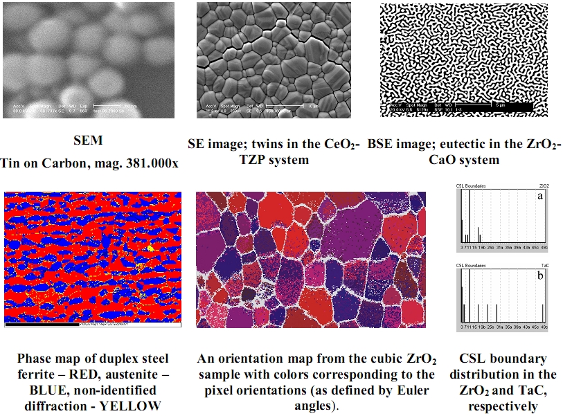
Microstructure investigations in Scanning Electron Microscopy Laboratory
Equipment and Analytical CapabilitiesEquipment:
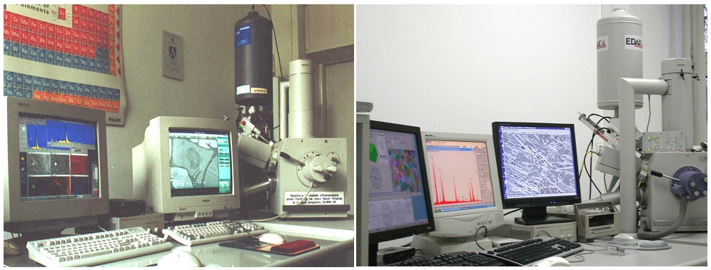
I. Conventional Scanning Electron Microscope PHILIPS XL30 (SEM) + Energy Dispersive X-Ray Spectrometer (EDXS) LINK ISIS
The XL30 Conventional Scanning Electron Microscope (CSEM) manufactured by Philips Electron Optics is used for surface observations of a wide range of conductive or non-conductive solid state samples (the latter analyzed after C or Au evaporation). A guaranteed
point resolution of 3.5 nm at 30 kV and 30 nm at 1 kV is achieved; the continuously variable accelerating voltage covers the range from 0.2 kV to 30 kV and the magnification range changes from 10x to 400.000x. Scan modes are either full frame, reduced raster (beam scans
in a limited area), horizontal line scan or spot mode.
The Energy Dispersive X-ray Spectrometer (EDXS) manufactured by Oxford Instruments, fully integrated with the SEM XL30, offers qualitative and quantitative elemental analysis of all elements down to boron (Z = 5). Images, spectra and X-ray maps from analyzed
microareas can be acquired. Two data correction procedures are available on the EDX LINK ISISi.e. ZAF and PhiRoZet. The first procedure gives excellent results for elements Z>11, while the second one is used especially for the light elements at low electron beam energies.
The X-ray Si(Li) Pentafet detector with energy resolution of 138 eV operates with Super Ultra Thin Window (SUTW) for the ultimate in light elements performance.
II. Environmental Scanning Electron Microscope FEI XL30 (E-SEM) + Energy Dispersive X-Ray Spectrometer EDAX Genesis 4000 + EBSD system (Oxford Instruments, previous HKL Technology)
The E-SEM XL30 Environmental Scanning Electron Microscope manufactured by FEI Company is used for surface observations of a wide range of inorganic and organic samples both in High and Low Vacuum mode. It allows to analyze the surface morphology without ANY coating with might obscure or damage outermost layes of the observed specimen. A guaranteed point resolution of 3.5 nm at 30 kV and 30 nm at 1 kV is achieved; the continuously variable accelerating voltage covers the range from 0.2 kV to 30 kV and the
magnification range changes from 10x to 500.000x. Gas pressure range changes from 0.1 to 20 torr; different gases (incl. water vapour) are available. Scan modes are either full frame, reduced raster (beam scans in a limited area), horizontal line scan or spot mode.
Electron Backscatter Diffraction (EBSD) is applied to examine a wide range of crystalline materials and to measure microstructure, orientation, texture (microtexture) and boundary properties. It can also be used in conjunction with chemical analyses to identify
unknown phases. The EBSD CHANNEL 5 system made by the Oxford Instruments consists of: EBSD detector with integrated forescatter electron detectors, Flamenco - imaging, diffraction pattern acquisition and indexing software, Twist - phase reflector file generation
software, Project Manager - data management and analysis software, Tango - orientation mapping software and Mambo - pole figure software.
| Conventional Scanning Electron Microscope XL30 PHILIPS Electron Optics + EDXS | Environmental Scanning Electron Microscope E-SEM XL30 FEI + EDXS +EBSD |
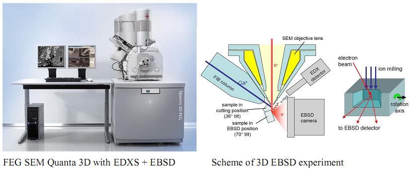
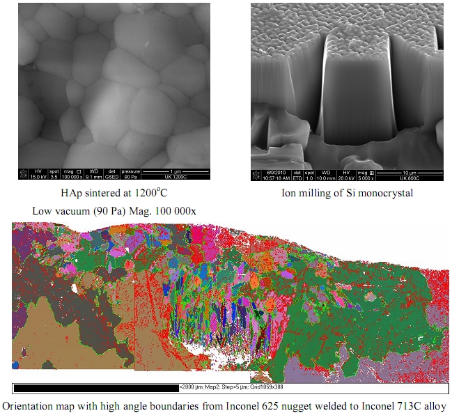
III. FEI QUANTA 3D FEG + EDAX Pegasus XM4i (High resolution scanning electron microscope FEI QUANTA 3D with high-brightness Schottky field emission source). The microscope is equipped with the following analytical facilities: Energy Dispersive X-Ray Spectrometer (EDXS) and Electron Backscatter Diffraction (EBSD) system. The microscope allows operating in three modes: High-vacuum, Low-vacuum and ESEM.. It enables imaging of any sample (metals, alloys, ceramics, polymers, organic materials, wet samples) and running EDXS and EBSD analysis of conductive and non-conductive sample. The microscope has the following parameters (the most important are listed below): Resolution at 30 kV - 1.2 nm for high vacuum and 1.5 nm for low-vacuum. Microscope is equipped with three detectors:
- secondary electron detector (Everhart-Thornley detector);
- gaseous secondary electron detector;
- solid state backscatter electron detector.
- accelerating voltage in the range from 2 kV to 30 kV;
- ion current beam in the range from 1 pA to 60 nA.
- point analysis;
- reduced scan;
- mapping;
- linescan.
- Morphology of nanomaterials
- Morphology and chemical composition of non-conductive samples in low vacuum
- Orientation topography of fine grain crystallographic materials with complete phase identification
- 3-dimentional analysis of morphological features, chemical elements distribution and crystallographic parameters
- Simultaneous chemical (EDXS) and crystallographic (EBSD) analysis from the same area
- In-situ crystallographic orientation analysis and phase transformation observations by use of heating stage and cooling stage (Peltier stage)
back