


Microstructure investigations in Scanning Electron Microscopy Laboratory
Examples of orientation topography studies in TEM and SEM Orientation mapping techniques and their role in characterization of microstructures
Examples of orientation topography studies in TEM and SEM Orientation mapping techniques and their role in characterization of microstructures Electron Backscatter Diffraction (EBSD) is a technique which allows crystallographic information to be obtained from samples in the scanning electron microscope (SEM). Application of EBSD to analyze microstructure and microtexture of metals and alloys has been widely exploited since the middle of nineties of the last century when the systems to acquire Automatic Crystal Orientation Maps (ACOM) have been commercially available. Capabilities of this technique seem to be extremely powerful. Microstructure can be quantitatively characterized, different phases identified and grain boundary character and morphology described. Crystal orientation and misorientation distributions in microscopic and mezoscopic scale can also be evaluated. This technique has shown in the last decade a spectacular advance in speed and quality of the data as well as post-processing procedures.During last couple of years Orientations Mapping (OM), i.e. determination of topography of crystallite orientations, has become a well established technique for studying and quantifying microstructures. The OM can be used for quantitative description of microstructure of each mono- and polycrystalline material. At present, due to the progress in automation of the diffraction measurements, especially in the Scanning Electron Microscope (SEM), Electron BackScattered Diffraction (EBSD) is extensively applied for acquiring orientations maps. The techniques of OM are also being developed in the Transition Electron Microscope (TEM), where Transmission Kikuchi Patterns (TKP) and Convergent Beam Electron Diffraction (CBED) have been successfully introduced for creating such maps. Orientation mapping can be performed both in the TEM and SEM with a spatial resolution in the range from several to hundreds of nanometers, respectively.
Three selected applications show the importance of the OM in characterizing materials properties, mainly:
a) deformation and recrystallization behavior of Face Centre Cubic (FCC) single crystals;
b) description of microstructure in highly cold-rolled aluminum alloy 6013;
c) orientation relationships between grains of different phases in ceramic composites.
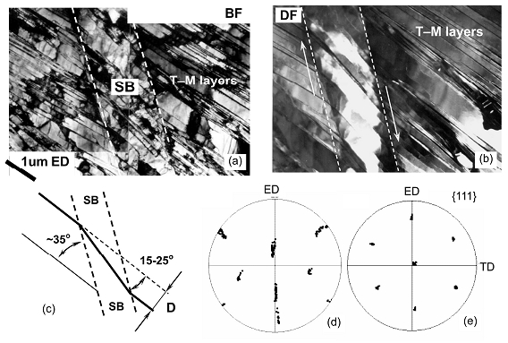
Ad a) Throughout this study the microstructural evolution during deformation and light annealing single crystals of a FCC metals have been characterized by detailed local orientation measurements before and after annealing to partial recrystallization. The main goal of this work is to understand the formation mechanism of new grain orientations in the early stages of recrystallization in low Stacking Fault Energy (SFE) metals, paying particular attention to the specific microtexture components of Shear Bands (SB). Substantial progress in understanding the formation of the bands was possible thanks to systematic local orientation measurements using particularly the TEM. TEM orientation maps allowed investigation of the way in which unstable behavior of strongly anisotropic layers leads to the SBs. It has been found also that several important transitions of the deformation textures are correlated with shear banding. The presence of characteristic directions as rotation axes in the process of primary nuclei formation suggests a close link with the deformation process (Fig. 1).
Ad b) The microstructure of cold rolled 6013 aluminum alloy is strongly inhomogeneous. In the laminar matrix large (>1ľm) particles of the second phase with zones of localized strain around are dispersed. Local crystallographic orientation distributions in such regions, determined by measurement of crystallographic orientations in the TEM differ significantly from the global deformation texture. Strong dispersed orientations in the zones tends to form groups in the areas of deformation components after rotation about the TD or/and Normal Direction (ND). From the calorimetric investigations and local orientation measurements in the SEM it has been concluded that recrystallization can be considered as series, partly overlapping, processes occurring in two major steps. At the first step, Particle Stimulated Nucleation (PSN) and some enlargement of new grains in the directions of low orientation gradient (mainly in the sheet plane) takes place. Newly formed grains often have a plate-like habit with shorter axis parallel to the ND. The orientations of the PSN grains reproduce roughly those which had been measured at deformed stage around large particles. At the second step, the growth of new grains in the direction of highly oriented gradient (the ND in this case) has been observed. The growth has been limited by distances between large particles along the ND (Figs 2-4).
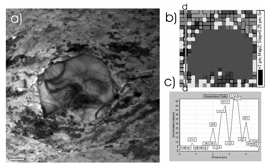
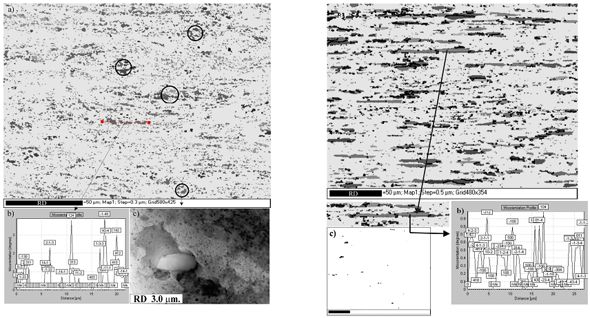
| Fig. 3. Microstructure of 6013 alloy, 75% cold rolled and subsequently heated in the calorimeter to 3300C, longitudinal section,SEMFEG/EBSD. A) Orientation topography in areas of the new grains, deformed regions - light grey, b) Disorientation profile along the a-a line, c) Microstructure around large particle of the second phase. | Fig. 4. Microstructure of 6013 alloy, 75% cold rolled and subsequently heated in the calorimeter to 3500C, longitudinal section, SEM/FEG. A) Orientation topography in areas of the new grains, deformed regions are bright gray, b) Example of disorientation profile along RD, c) Topography of new grains with orientations close to the Cube position. |
In above cases the investigated samples are conductive. Thus, the operator encounters no problems connected with specimen charging. However, the situation changes dramatically when poorly conductive samples are analyzed in the SEM. Controlling the charge and quality of the surface are the challenges for the operator running experiments on insulators. Specimen charging obscures both the forward scatter electrons image and decreases the EBSD pattern quality making its analysis difficult or even impossible. Also final steps of sample preparation largely determine whether or not the pattern quality is sufficient for indexing. The influence of several important parameters, e.g. gas pressure, a type of gas, working distance and energy of electron beam on the EBSD pattern quality must be taken into consideration by the operator. The coupling of crystallographic information with the chemical data obtained from Energy Dispersive Spectroscopy (EDS) in the Low Vacuum (LV-SEM) will show that it is also possible to perform phase identification of insulators.
Ad c) The microstructure of ceramic composites and their mechanical properties can be better understood by investigating crystallographic relationships between several adjacent grains. To establish such correlations the EBSD has been successfully introduced providing information about relative orientations of crystals. By applying this technique in the LV-SEM with a large number of diffraction patterns from several hundreds of neighboring grains can be collected, indexed and stored during one single experiment. Then, orientation relationships between several or even hundreds of grains of non-conductive ceramics can be established giving a sufficient ground for general characteristics of the material under investigation.
Such an experiment was illustrated with the results carried out on non-conductive ceramics such as: (PbLa)(ZrTi)O3 ceramics (Fig.5), alumina and zirconia based composites reinforced with different carbides as well as alumina ceramics which underwent a special surface treatment, i.e. shot peening. - a process used to modify mechanical properties of surface layers in metals and ceramics by impacting a surface with shot with force sufficient to create plastic deformation (Fig.6).
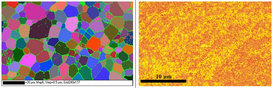
| Fig. 5. Orientation map acquired from the PLZT ceramics. Note that the total number of indexed diffractions exceeded 91.6%. | Fig. 6. Deformation map acquired from alumina showing the areas of different dislocation densities |
back